
Существуют схемы усилителей НЧ, передатчиков, других устройств, которые требуют питания не только от двуполярного источника, но и от двух гальванически развязанных источников, не имеющих соединения с «землей» или общих связанных цепей. Организовать питание такого устройства в стационарных условиях весьма просто, так как источником питания служит электросеть, а значит будет силовой или импульсный трансформатор. Достаточно сделать две вторичные обмотки, не соединенные с другими цепями, и переменные напряжения с них подать на отдельные независимые выпрямители.
Сложнее организовать питание от двух гальванически развязанных источников, если источником питания должен служить источник постоянного тока, например, бортовая сеть автомобиля или катера.
На рисунке ниже представлена схема импульсного обратноходового источника, на выходе которого имеется два гальванически развязанных напряжения 15V, с максимально допустимым током по 1А. Если необходимо обычное двуполярное питание эти выходы можно соединить последовательно, — плюс одного с минусом другого, а точка соединения будет общим нулевым проводом.
Схема ставшая уже стандартной, — источник постоянного тока, импульсный генератор, импульсный трансформатор, выпрямители во вторичных цепях.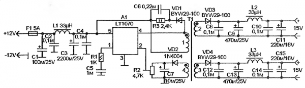
Напряжение 12V от автомобильного аккумулятора поступает на микросхему А1 типа L.T1070 (обратноходовый DC-DC преобразователь). Цепь C1-C2-L1-C3-C4 заграждает путь помехам, которые могут проникать из систем автомобиля или катера.
Микросхема А1 формирует импульсы частотой около 40 kHz. На выходе микросхемы есть ключ, выведенный на вывод 4. Он нагружен первичной обмоткой импульсного трансформатора Т1. Цепь C6-R3-VD1 ограничивает отрицательные выбросы в обмотке.
Во вторичных обмотках наводится ЭДС. Обмотка 4 является контрольной. Переменное напряжение на ней выпрямляется диодом VD2 и через подстроечный резистор R2 поступает на контрольный вход микросхемы А1 (вывод 2). Система стабилизации выходного напряжения LN1070 работает таким образом, что контроллер микросхемы изменяет скважность импульсов на выводе 4 таким образом, чтобы напряжение на выводе 2 было равно 1,24V. То есть, чтобы получить стабилизацию напряжения нужно снять напряжение с вторичной цепи и через делитель на резисторах подать его на вывод 2. Соотношение плеч делителя должно быть таким чтобы при нормальном напряжении на выходе, на выводе 2 было 1,24V. В данной схеме снимать напряжения для системы стабилизации с выхода нежелательно, так как изначально поставлена цель создания источника с гальванически развязанными выходными напряжениями как друг от друга, так и от первичных цепей. Поэтому здесь есть третий вторичный источник, состоящий из обмотки 4 и выпрямителя VD2-C7. Он служит только для получения контрольного напряжения. Так как обмотка 4 в составе трансформатора, то напряжение на ней в такой же зависимости от скважности импуль-сов, как и напряжения на других обмотках.
Трансформатор Т1 намотан на ферритовом кольце диаметром28 мм. Первичная обмотка содержит 40 витков провода ПЭВ 0.47. Она наматывается первой Затем, на неё, в том же направлении нужно намотать вторичные обмотки 2 и 3. Берут такой же провод и сложив его вдвое наматывают 50 витков. Обмотка 4 — в том же направлении что и остальные, -10 витков ПЭВ — 0,12.
Налаживание сводится к установке выходного напряжения подстройкой R2.
Источник: Л.Кузянский, Радиоконструктор, 05-2010.
Источник
Самодельный преобразователь напряжения 12В в 19В для ноутбука (LT1070)
Принципиальная схема самодельного преобразователя напряжения DC-DC для питания ноутбуков от источников с напряжением 12В. Напряжение питания ноутбука Toshiba-Satellite составляет 19V примаксимальном токе ЗА. К сожалению, это совсем не подходит для работы в автомобиле, так как там 12V.
Принципиальная схема
На рисунке в тексте приведена схема преобразователя напряжения, повышающего автомобильные 12V до ноутбуковских 19V, и поддерживающего это напряжение стабильным. В основе схемы DC-DC-преоб-разователь на микросхеме LT1070.
Напряжение от бортовой сети автомобиля через 5-амперный предохранитель и помехоподавляющие цепи поступает на точку подачи питания микросхемы А1 (вывод 5) Генератор микросхемы начинает работать и подавать импульсы на ключ, имеющийся в А1, включенный между выводом 4 и общим минусом (выв. 3).
Ключ периодически открываясь пропускает импульсный ток через первичную обмотку трансформатора Т1. Во вторичной обмотке Т1 наводится переменное напряжение, которое выпрямляется диодом VD2 и сглаживается емкостями С9, С10. Далее через цепь L2-C11-C12 постоянное напряжение 19V поступает на выход источника.
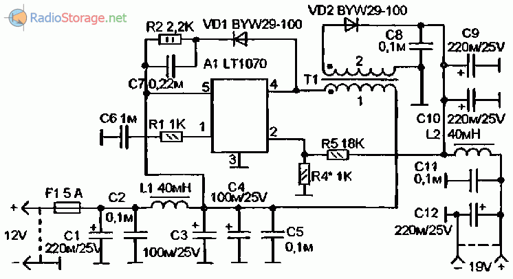
Рис. 1. Принципиальная схема DC-DC преобразователя напряжения для питания ноутбука от 12В.
Для контроля уровня выходного напряжения и его стабилизации используется внутренняя схема стабилизации А1. Суть ее работы в том, что она таким образом изменяет скважность импульсов, поступающих на первичную обмотку трансформатора, чтобы на выводе 2 А1 было постоянное напряжение 1,24V.
Для получения стабильного выходного напряжения нужно с выхода вторичного выпрямителя на VD2 постоянное напряжение через делитель подать на вывод 2 А1. А соотношение резисторов делителя должно быть таким, чтобы при правильном напряжении на выходе, на выводе 2 А1 было напряжение 1,24V. Резисторы делителя это R5 и R4. Точным подбором R4 устанавливают требуемое номинальное стабилизированное выходное напряжение. В данном случае, это 19V.
Детали и печатная плата
Для намотки трансформатора взято ферритовое кольцо внешним диаметром 32 мм. из феррита 2000НМ. Кольцо нужно обернуть тонким слоем фторопластовой пленки или лакоткани. Можно кольцо ничем не оборачивать, а покрытъ слоем эпоксидного лака. После его высыхания можно наматывать обмотки.
Вполне возможно, что для намотки трансформатора можно использовать и кольцо отличающегося диаметра и марки феррита, — нужно экспериментировать!
Первичная обмотка содержит 40 витков обмоточного провода, состоящего из двух вместе сложенных проводов ПЭВ 0,43. Можно использовать и одинарный провод сечением 0,*, но наматывать будет сложнее. Вторичная обмотка содержит 70 витков такого же двойного провода. Сначала наматывают первичную обмотку, а затем на её поверхность вторичную, укладывая провод в том же направлении, что и наматывали первичную. На схеме начала обмоток трансформатора отмечены точками.
Для дросселей используются кольца диаметром 18-20 мм. Они содержат по 30 витков такого же двойного провода, как и для намотки трансформатора. Схема преобразователя собрана на печатной плате с односторонним расположением печатных дорожек.
Микросхему и диоды необходимо укрепить на радиаторах. Общим радиатором может служить металлический корпус, в котором собран преобразователь (на плате диоды и микросхема специально расположены у края).
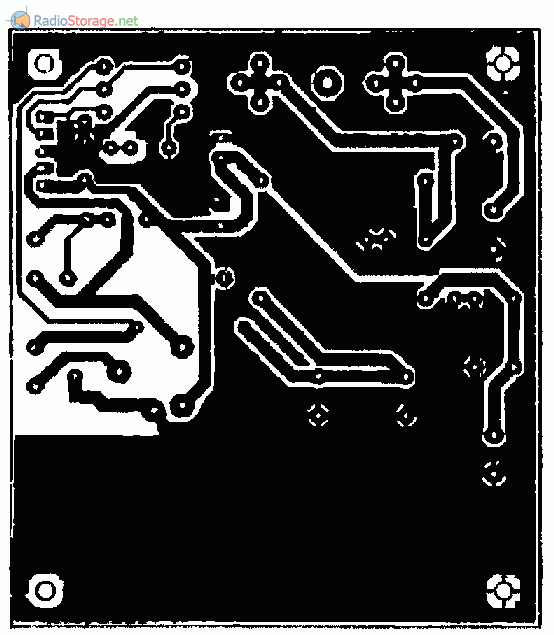
Рис. 2. Печатная плата схемы DC-DC преобразователя напряжения для ноутбука.
Микросхему можно установить на радиатор-корпус с использованием теплопроводной пасты, не изолируя, так как её радиаторная пластина соединена с 3-м выводом, а он с общим минусом (с «землей»). А диоды на радиатор нужно ставить через слюдяные прокладки на теплопроводной пасте, используя эбонитовые шайбы, так чтобы обеспечить изоляцию их катодных пластин от корпуса.
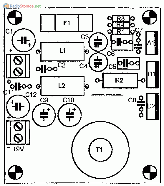
Рис. 3. Расположение деталей на плате преобразователя напряжения для ноутбука.
Налаживание
При правильном монтаже и исправных деталях налаживание сводится к проверке выходного напряжения. Если оно отличается от необходимого нужно изменить сопротивление резистора R4. Уменьшение сопротивления ведет к повышению напряжения, а увеличение к его понижению. Операцию замены резистора нужно делать только после выключения питания.
Поэтому, временно его можно заменить переменным сопротивлением 1,5-2,5 kOm. С помощью него нужно установить необходимое выходное напряжение, проверить на нагрузке, например, подключив лампу накаливания на 36V (или две последовательно включенные автомобильные лампочки как для задних фонарей).
После того как настройка будет завершена нужно, после выключения питания, отпаять переменный резистор и измерить его сопротивление. Затем установить на плату постоянный резистор такого сопротивления или очень близкого к полученному. Возможно, необходимого номинала не окажется и потребуется набрать R4 из нескольких резисторов используя последовательное или параллельное включение.
Включать преобразователь без теплоотвода под микросхему А1 рискованно, поэтому, даже в процессе налаживания, особенно при испытании на нагрузке, нужно установть её на какой-нибудь радиатор и периодически контролировать температуру. Этот же преобразователь можно использовать и для питания других приборов от бортовой сети автомобиля. Нужное выходное напряжение устанавливают подбором резисторов R5-R4 и числа витков вторичной обмотки трансформатора.
Источник
Datasheet Linear Technology LT1070 — Даташит
5A and 2.5A High Efficiency Switching Regulators
Datasheets
LT1070/LT1071 5A and 2.5A High Efficiency Switching Regulators DESCRIPTIO U FEATURES ■ ■ ■ ■ ■ ■ ■ ■ ■ ■ Wide Input Voltage Range: 3V to 60V Low Quiescent Current: 6mA Internal 5A Switch (2.5A for LT1071) Very Few External Parts Required Self Protected Against Overloads Operates in Nearly All Switching Topologies Shutdown Mode Draws Only 50µA Supply Current Flyback Regulated Mode Has Fully Floating Outputs
Comes in Standard 5-Pin TO-220 Package …
| Производитель | Linear Technology |
| Серия | LT1070 |
Корпус / Упаковка / Маркировка
Параметры
| Код корпуса | T | T | T | T | T |
| Индекс корпуса | 05-08-1421 (Flow 06) | 05-08-1421 (Std) | 05-08-1421 (Std) | 05-08-1421 (Flow 06) | 05-08-1421 (Std) |
| Количество выводов | 5 | 5 | 5 | 5 | 5 |
| Parameters / Models | LT1070CT#06PBF | LT1070CT#30PBF | LT1070CT#PBF | LT1070IT#06PBF | LT1070IT#PBF |
|---|---|---|---|---|---|
| Design Tools | LTspice Model | LTspice Model | LTspice Model | LTspice Model | LTspice Model |
| Экспортный контроль | нет | нет | нет | нет | нет |
| Тактовая частота, kHz | 40 | 40 | 40 | 40 | 40 |
| Ishutdown, мкА | 100 | 100 | 100 | 100 | 100 |
| Isupply, мА | 6 | 6 | 6 | 6 | 6 |
| Monolithic | да | да | да | да | да |
| Количество выходов | 1 | 1 | 1 | 1 | 1 |
| Рабочий диапазон температур, °C | от 0 до 70 | от 0 до 70 | от 0 до 70 | от -40 до 85 | от -40 до 85 |
| Switch Current, A | 5 | 5 | 5 | 5 | 5 |
| Synchronous | нет | нет | нет | нет | нет |
| Topology | Boost, Flyback, Sepic | Boost, Flyback, Sepic | Boost, Flyback, Sepic | Boost, Flyback, Sepic | Boost, Flyback, Sepic |
| Vin Max, В | 40 | 40 | 40 | 40 | 40 |
| Vin Min, В | 3 | 3 | 3 | 3 | 3 |
| Vin Min Startup, В | 3 | 3 | 3 | 3 | 3 |
| Vout Max, В | 40 | 40 | 40 | 40 | 40 |
| Vout Min, В | 1.244 | 1.244 | 1.244 | 1.244 | 1.244 |
| Vswitch Max, В | 65 | 65 | 65 | 65 | 65 |
Экологический статус
Другие варианты исполнения
Application Notes
Application Note 19 June 1986 LT1070 Design Manual Carl Nelson INTRODUCTION Three terminal monolithic linear voltage regulators appeared almost 20 years ago, and were almost immediately successful for a variety of reasons. In particular, there were relatively few engineers capable of designing a good linear voltage regulator. The new devices were also easy to use, and inexpensive. In currently popular parlance they were «expert systems,» containing a good deal of their designer’s knowledge in silicon form. Because of these advantages, the regulators quickly eclipsed discrete and earlier monolithic building blocks and dominated the market. More recently, there has been increasing interest in switching-based regulators. Switching regulators, with their high efficiency and small size, are increasingly desirable as overall package sizes have shrunk. Unfortunately, switching regulators are also one of the most difficult linear circuits to design. Mysterious modes, sudden failures, peculiar regulation characteristics and just plain explosions are common occurrences during the design of a switching regulator. Most switching regulator ICs are building blocks. Many
discrete components are required, and substantial expertise is assumed on the part of the user. Some newer …
Application Note 25September 1987 Switching Regulators for PoetsA Gentle Guide for the TrepidatiousJim WilliamsThe above title is not happenstance and was arrived at afterconsiderable deliberation. As a linear IC manufacturer, it isour goal to encourage users to design and build switchingregulators. A problem is that while everyone agrees thatworking switching regulators are a good thing, everyonealso agrees that they are difficult to get working. Switchingregulators, with their high efficiency and small size, areincreasingly desirable as overall package sizes shrink.Unfortunately, switching regulators are also one of themost difficult linear circuits to design. Mysterious modes,sudden, seemingly inexplicable failures, peculiar regulation characteristics and just plain explosions are commonoccurrences. Diodes conduct the wrong way. Things gethot that shouldn’t. Capacitors act like resistors, fusesdon’t blow and transistors do. The output is at ground, andthe ground terminal shows volts of noise.Added to this poisonous brew is the regulator’s feedbackloop, sampled in nature and replete with uncertain phaseshifts. Everything, of course, varies with line and load
conditions— and the time of day, or so it seems. In the face …
Application Note 29October 1988Some Thoughts on DC/DC ConvertersJim Williams and Brian HuffmanINTRODUCTIONMany systems require that the primary source of DC powerbe converted to other voltages. Battery driven circuitry isan obvious candidate. The 6V or 12V cell in a laptop computer must be converted to different potentials needed formemory, disc drives, display and operating logic. In theory,AC line powered systems should not need DC/DC convertersbecause the implied power transformer can be equippedwith multiple secondaries. In practice, economics, noiserequirements, supply bus distribution problems and otherconstraints often make DC/DC conversion preferable. Acommon example is logic dominated, 5V powered systemsutilizing ±15V driven analog components.The range of applications for DC/DC converters is large,with many variations. Interest in converters is commensurately quite high. Increased use of single supply poweredsystems, stiffening performance requirements and batteryoperation have increased converter usage.Historically, efficiency and size have received heavy emphasis. In fact, these parameters can be significant, butoften are of secondary importance. A possible reason
behind the continued and overwhelming attention to size …
Application Note 30February 1989Switching Regulator Circuit CollectionJohn SeagoSwitching regulators are of universal interest. LinearTechnology has made a major effort to address this topic.A catalog of circuits has been compiled so that a designengineer can swiftly determine which converter type isbest. This catalog serves as a visual index to be browsedthrough for a specific or general interest. The catalog is organized so that converter topologies canbe easily found. There are 12 basic circuit categories:Battery, Boost, Buck, Buck-Boost, Flyback, Forward, HighVoltage, Multioutput, Off Line, Preregulator, SwitchedCapacitor and Telecom. Additional circuit information canbe located in the references listed in the index. Thereference works as follows, i.e., AN8, Page 2 = ApplicationNote 8, Page 2; LTC1044 DS = LTC1044 data sheet;DN17 = Design Note 17. DRAWING INDEXFIGURE TITLE FIGURE # PAGE REFERENCE/SOURCE Battery2A Converter with 150ВµA Quiescent Current (6V to 12V)200mA Output Converter (1.5V to 5V)Up Converter (6V to 15V)
Regulated Up Converter (5V to 10V) …
Application Note 35August 1989Step-Down Switching RegulatorsJim Williamslost in this voltage-to-current-to-magnetic field-to-current-to-charge-to-voltage conversion. In practice, thecircuit elements have losses, but step-down efficiency isstill higher than with inherently dissipative (e.g., voltagedivider) approaches. Figure 2 feedback controls the basiccircuit to regulate output voltage. In this case switch ontime (e.g., inductor charge time) is varied to maintain theoutput against changes in input or loading.REGULATEDOUTPUT IN PULSEWIDTHMODULATOR Figure 1 is a conceptual voltage step-down or “buck”circuit. When the switch closes the input voltage appearsat the inductor. Current flowing through the inductor-capacitor combination builds over time. When the switchIN OUT AN35 F01 Figure 1. Conceptual Voltage Step-Down (“Buck”) Circuit opens current flow ceases and the magnetic field aroundthe inductor collapses. Faraday teaches that the voltageinduced by the collapsing magnetic field is opposite to theoriginally applied voltage. As such, the inductor’s left sideheads negative and is clamped by the diode. The capacitors accumulated charge has no discharge path, and a DCpotential appears at the output. This DC potential is lower
than the input because the inductor limits current during …
Application Note 39February 1990Parasitic Capacitance Effectsin Step-Up Transformer DesignBrian HuffmanOne of the most critical components in a step-up designlike Figure 1 is the transformer. Transformers have parasitic components that can cause them to deviate fromtheir ideal characteristics, and the parasitic capacitanceassociated with the secondary can cause large resonatingcurrent spikes on the leading edge of the switch currentwaveform. These spikes can cause the regulator to exhibiterratic operating conditions that manifests itself as dutycycle instability. This effect is exacerbated in very highvoltage designs. Attention to transformer design will curethis problem. Figure 2 shows the high frequency current paths of theparasitic capacitors. In the analysis of operation assumethe input and output voltages are at AC ground. Thus, theparasitic capacitors are all in parallel. The transformer’ssecondary provides the AC current path for these capacitors. The current flowing through the secondary producesN times the current in the primary. As the parasitic capacitance and turns ratio increase, the primary currentbecomes progressively larger. D1MUR1100
VIN …
Application Note 44September 1991LT1074/LT1076 Design ManualCarl NelsonINTRODUCTIONThe use of switching regulators increased dramatically inthe 1980’s and this trend remains strong going into the90s. The reasons for this are simple; heat and efficiency.Today’s systems are shrinking continuously, while simultaneously offering greater electronic “horsepower.” Thiscombination would result in unacceptably high internaltemperatures if low efficiency linear supplies were used.Heat sinks do not solve the problem in general becausemost systems are closed, with low thermal transfer from“inside” to “outside.”Battery-powered systems need high efficiency supplies forlong battery life. Topological considerations also requireswitching technology. For instance, a battery cannotgenerate an output higher than itself with linear supplies.The availability of low cost rechargeable batteries has created a spectacular rise in the number of battery-poweredsystems, and consequently a matching rise in the use ofswitching regulators.The LT®1074 and LT1076 switching regulators are designed
specifically for ease of use. They are close to the ultimate …
Design Notes
advertisement Achieving Microamp Quiescent Current in Switching RegulatorsDesign Note 11Jim WilliamsMany battery powered applications require very wideranges of power supply output current. Normal conditions require currents in the ampere range, whilestandby or “sleep” modes draw only microamperes.A typical lap top computer may draw 1 to 2 amperesrunning while needing only a few hundred microampsfor memory when turned off. In theory, any switchingregulator designed for loop stability under no-loadconditions will work. In practice, a regulator’s relativelylarge quiescent current may cause unacceptable batterydrain during low output current intervals.Figure 1 shows a typical flyback regulator. In thiscase the 6V battery is converted to a 12V output bythe inductive flyback voltage produced each time theLT®1070’s VSW pin is internally switched to ground. Aninternal 40kHz clock produces a flyback event every25μs. The energy in this event is controlled by the IC’sinternal error amplifier, which acts to force the feedback(FB) pin to a 1.23V reference. The error amplifiers highimpedance output (the VC pin) uses an RC damper for
stable loop compensation. …
Telephone Ring-Tone Generation – Design Note 134Dale EagarRequirementsWhen your telephone rings, exactly what is the phonecompany doing? This question comes up frequently, asit seems everyone is becoming a telephone company.Deregulation opens many new opportunities, but if youwant to be the phone company you have to ring bells.An Open-Architecture Ring-Tone GeneratorHere is a design that you can own, tailor to your specificneeds, layout on your circuit board and put on your billof materials. Finally, you will be in control of the blackmagic (and high voltages) of ring-tone generation.Not Your Standard Bench SupplyRing-tone generation requires not one but two highvoltages, 60VDC and – 180VDC (this arises from theneed to put 87VRMS on –48VDC). Figure 1 details theswitching power supply that delivers the volts neededto run the ring-tone circuit. This switcher can be powered from any voltage from 5V to 30V and shuts downwhen not in use. Figure 2 is the build diagram of thetransformer used in the switching power supply.60V
MUR160 = PRIMARY GROUND T1 2 = SECONDARY GROUND + …
A Battery Powered Lap Top Computer Power SupplyDesign Note 18Brian HuffmanMost battery powered lap top computers require regulated multiple output potentials. Problems associatedwith such a supply include magnetic and snubber design,loop compensation, short circuit protection, size andefficiency. Typical output power requirements include5V @ 1A for memory and logic circuitry and ±12V@ 300mA to drive the analog components. Primarypower may be either a 6V or 12V battery. The circuitin Figure 1 meets all these requirements. The LT®1071simplifies the power supply design by integrating mostof the switching regulator building blocks. Also, theoff-the-shelf transformer eliminates all the headachesassociated with the magnetic design.The circuit is a basic flyback regulator. The transformertransfers the energy from the 12V input to the 5V and±12V outputs. Figure 2 shows the voltage (trace A) andthe current (trace B) waveforms at the VSW pin. TheVSW output is a collector of a common emitter NPN,so current flows through it when it is low. The circuit’s40kHz repetition rate is set by the LT1071’s internal
oscillator. During the VSW (trace A) “on” time, the input …
advertisement Floating Input Extends Regulator Capabilities – Design Note 21Brian Huffmanhowever, if the secondary windings are isolated fromone another, a low dropout positive voltage regulatorcan be used for negative regulation (Figure 1). Many applications require circuit performance that isunachievable with conventional regulator design. Thisresults in added complexity to the circuit. However, someproblems can easily be solved by floating the input tothe regulator. A floating input can either be a battery, ora secondary winding that is galvanically isolated fromall other windings. With this method high efficiencynegative voltage regulation, high voltage regulation, andlow saturation loss positive buck switching regulatorcan all be achieved easily. In this circuit the LT®1086 servos the voltage betweenthe output and the adjust pin to 1.25V. The positiveregulation is accomplished by conventional regulatordesign. Negative voltage regulation is achieved byconnecting the output of the positive voltage regulatorto ground. The VIN pin floats to 1.5V or greater, aboveground. This technique can be used with any positivevoltage regulator, although highest efficiency occurswith low dropout types. Low dropout negative voltage regulators are not currently available. This would seem to preclude high efficiency negative linear regulators. Such regulation is
frequently desired in switching supply post regulators; L, LT, LTC, LTM, Linear Technology and the Linear logo are registered trademarks …
advertisement Inductor Selection for Switching RegulatorsDesign Note 8Jim WilliamsA common problem area in switching regulator designis the inductor, and the most common difficulty issaturation. An inductor is saturated when it cannothold any more magnetic flux. As an inductor arrivesat saturation it begins to look more resistive and lessinductive. Under these conditions current flow is limitedonly by the inductor’s DC copper resistance and thesource capacity. This is why saturation often resultsin destructive failures.While saturation is a prime concern, cost, heating,size, availability and desired performance are alsosignificant. Electromagnetic theory, although applicableto these issues, can be confusing, particularly to thenon-specialist.Practically speaking, an empirical approach is often agood way to approach inductor selection. It permits real time analysis under actual circuit operating conditionsusing the ultimate simulator—a breadboard. If desired,inductor design theory can be used to augment orconfirm experimental results.
Figure 1 shows a typical flyback regulator utilizing the …
Источник

Вам также может понравиться